
.png)
APE 2026 Highlights

APE 2026 Hightlights https://s46473.pcdn.co/wp-content/uploads/2026/02/2026.02.04-APE-Singapore-Day-31-1.mp4 View More
APE 2026 Gala Dinner

https://www.asiaphotonicsexpo.com/wp-content/uploads/2026/02/2026.02.04-APE-Singapore-Gala-Dinner1-2.mp4 View More
Day Two of APE 2026

https://www.asiaphotonicsexpo.com/wp-content/uploads/2026/02/2026.02.05-APE-Singapore-Day-21-1.mp4 View More
Day One of APE 2026
https://www.asiaphotonicsexpo.com/wp-content/uploads/2026/02/2026.02.04-APE-Singapore-Day-11-1.mp4 View More
Asia Photonics Expo 2026 Concludes in Singapore—Following three days of business and industry exchange
Singapore, 6 February 2026 – The third edition of the Asia Photonics Expo (APE) 2026 concluded today at the Sands Expo and Convention Centre, following three days of exhibitions, conferences and business engagement that brought together the global photonics and semiconductor ecosystem.
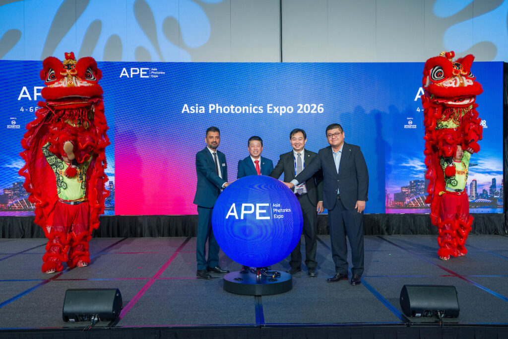
Asia Photonics Expo 2026 Opens in Singapore, Cementing Its Position as Asia’s Leading Photonics platform
The 3rd edition of the Asia Photonics Expo (APE) officially opened today at the Sands Expo and Convention Centre, convening the global photonics and semiconductor ecosystem for three days of networking, conferences, and industry collaboration from 4-6 February 2026.
Only One Week Left: Asia Photonics Expo 2026 Set to Unveil the Future of Photonics and Semiconductors in Singapore
Under the theme “Driving Innovation Where Photonics Meets Semiconductors,” APE 2026 will showcase leading technologies across optical communications, optics, semiconductors, lasers, infrared, sensing, and quantum technology. The event is expected to attract over 300 international exhibitors and 6,000 industry professionals, fostering a dynamic environment for discovery, collaboration, and business growth.
Breaking AI’s Bandwidth Barrier: Dr. Luo Xianshu on Silicon Photonics, Co-Packaged Optics, and Building Asia’s Innovation Ecosystem

In APE’s Photonics Spotlight series, Dr. Luo Xianshu shares his insights on how silicon photonics and co-packaged optics (CPO) are addressing AI interconnect bottlenecks, the ecosystem challenges for photonics heterogeneous integration (PHI), and the roadmap for emerging applications such as LiDAR, biosensing, and quantum computing. He also discusses NSTIC (Advanced Photonics) role in accelerating innovation and his outlook for Asia Photonics Expo 2026 as a catalyst for industry research collaboration.
Exclusive Interview with Dr. Wang Qian: Pioneering the Path from Laboratory to Wafer-Scale Metalens Innovation

In the following interview, Dr. Wang discusses recent revolutions in design and materials, critical fabrication hurdles, and the integration of metasurfaces with semiconductor platforms. She also highlights the strategic role of initiatives like Singapore’s National Semiconductor Translation and Innovation Centre (NSTIC) in accelerating the journey from research to commercialization, and shares her outlook on emerging applications and the unique value of platforms such as the Asia Photonics Expo in bridging research and industry.
Spotlight on Innovation: An Interview with Dr. Ramon Paniagua-Dominguez: Charting the Future of Metasurfaces and Integrated Photonics

In this latest edition of our Photonics Spotlight Series, we speak with Dr. Ramon Paniagua Dominguez, Principal Investigator at the Spanish National Research Council (CSIC), where he leads cutting-edge research in metasurfaces and flat optics. Previously based in Singapore at A*STAR for over a decade, Dr. Paniagua Dominguez has been at the forefront of developing programmable flat optics—work that continues to shape the future of nanophotonics and its applications.
Here, he shares his insights on technological trends, manufacturing challenges, and the collaborative future of global photonics innovation.